Semiconductor Fabrication
Semiconductor Fabrication — an illustrated inventions story, set in Global. 10 illustrated pages, free to read on Wonder Inventions.
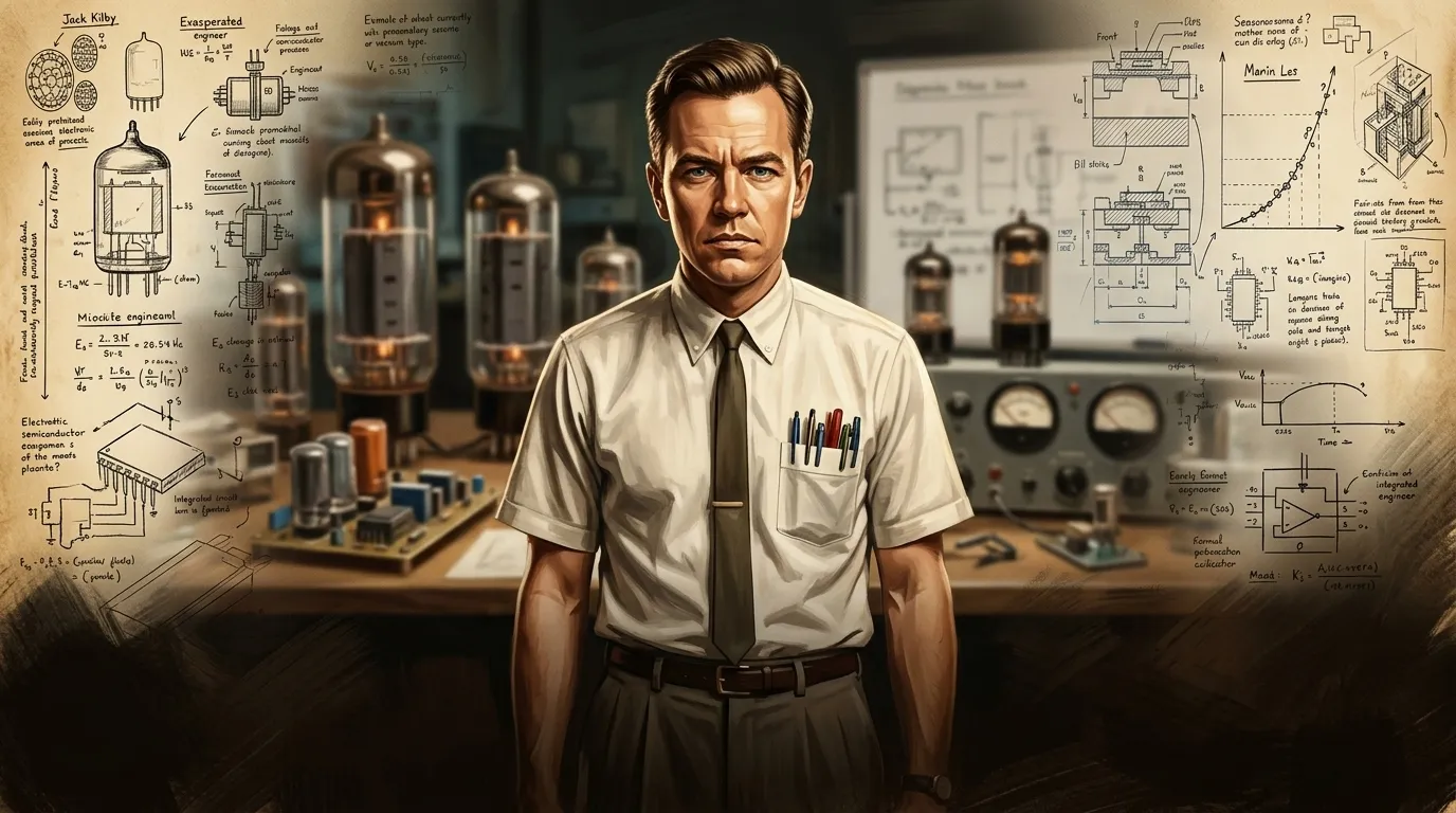
Page 1
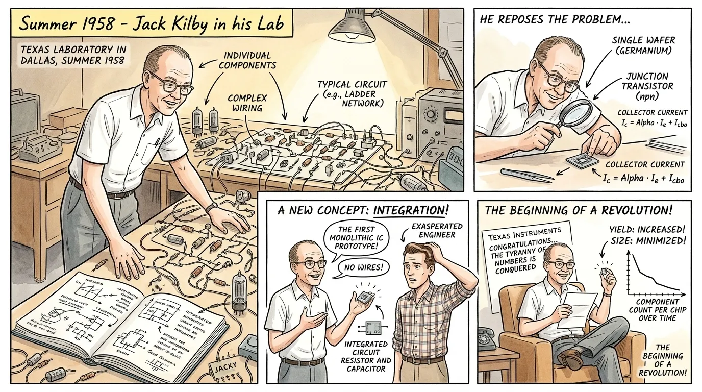
Before the integrated circuit, electronics relied on individual components—vacuum tubes and transistors—each manually wired, resulting in cumbersome and often unreliable machines. Engineers faced a profound bottleneck in miniaturization and assembly, limiting the reach of complex electronic systems. Yet, a vision for a radically different approach was emerging, spearheaded by determined innovators. The path to compact, powerful computing began with a simple, revolutionary idea.
"'This maze of wires... it's the very limit of our progress,' remarked Jack Kilby, a brilliant engineer at Texas Instruments in Dallas, contemplating a sprawling circuit board in the summer of 1958. 'We need to integrate everything, to make the circuit a single, indivisible entity.'"
Page 2
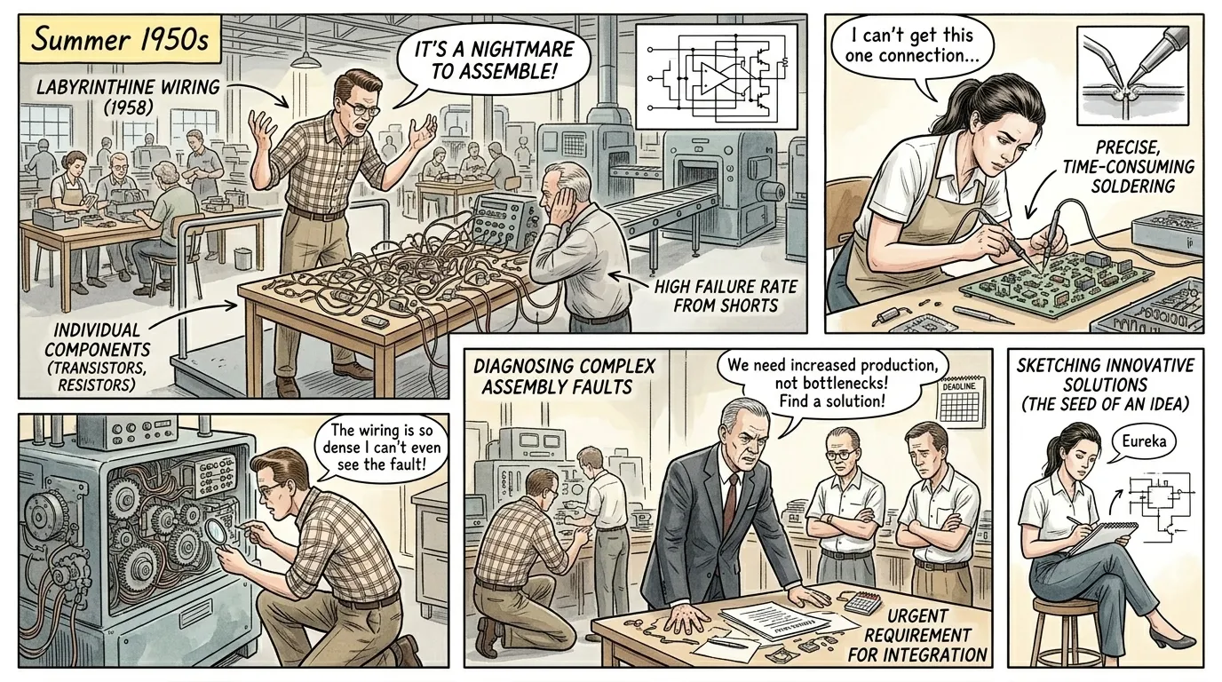
The demand for more sophisticated electronic devices in the mid-20th century exposed a critical flaw in existing manufacturing methods. Each new transistor or resistor required dedicated connections, leading to exponentially complex wiring, increased failure points, and prohibitive costs. The challenge was not just making components smaller, but reliably connecting thousands, then millions, of them. The physical limits of manual assembly loomed large, a genuine 'tyranny of numbers' for electrical engineers.
"An exasperated engineer, a man with short, slicked-back brown hair and a plaid shirt, threw his hands up in a bustling 1950s factory floor. 'Another failed connection! This rat's nest of individual components and miles of wire is simply impossible to mass-produce with any reliability!' he exclaimed to a colleague, a woman with a practical ponytail and a clean apron, meticulously soldering a connection on a crowded circuit board."
Page 3
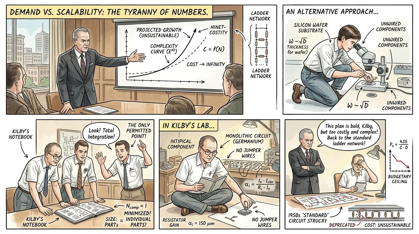
As computing power became a strategic imperative, driven by nascent space exploration and defense programs, the scalability crisis deepened. Enormous rooms were dedicated to computers powered by hundreds of thousands of individual components, consuming vast amounts of energy and generating immense heat. Every failure point in a manually assembled circuit represented downtime and expense, making the pursuit of integration not merely an ambition, but an urgent necessity for technological advancement. Early attempts to combine components still grappled with fundamental packaging issues.
"A stern-faced manager, a man in a crisp suit and tie, pointed emphatically at a projected growth chart during a tense 1950s boardroom meeting. 'Gentlemen, the demand for complex electronics is exploding, but our current methods won't scale. We must find a way to eliminate individual wires and solder joints,' he declared. 'Our current methods are simply not sustainable for the future we envision.'"
Page 4
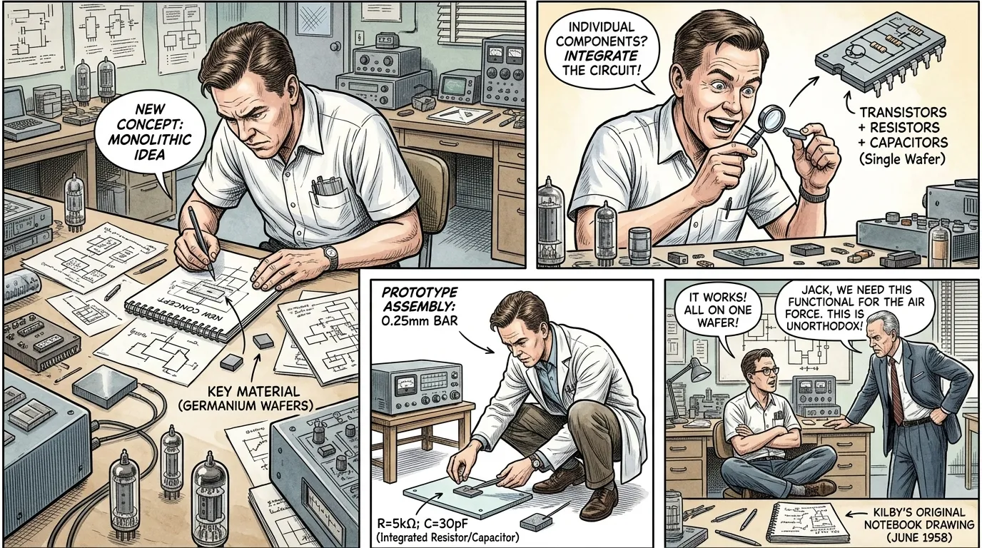
Jack Kilby, working without a summer vacation, pondered the problem of discrete components. He realized that all elements of a circuit – resistors, capacitors, and transistors – could theoretically be formed within a single block of semiconductor material. His breakthrough involved fabricating a tiny piece of germanium with these components already integrated, eliminating the need for separate wiring. This 'monolithic' concept, patented in 1959, was a conceptual leap, demonstrating that an entire circuit could exist as one indivisible entity.
"Alone in his lab during the quiet summer, Jack Kilby sketched furiously. He looked up, a spark of revelation in his eyes, and muttered, 'A single block. Everything in one piece. As Plato once suggested, 'necessity is the mother of invention,' and I feel the profound necessity for a better way to build circuits. This is it!'"
Page 5
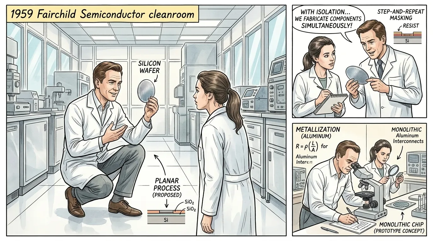
At Fairchild Semiconductor, just months after Kilby's initial breakthrough, Robert Noyce independently developed a complementary and equally vital innovation: the planar process. Noyce's method allowed for all circuit components to be diffused directly into the surface of a silicon wafer and then interconnected with a metal layer, all protected by a silicon oxide coating. This breakthrough addressed the crucial challenge of interconnections and provided a blueprint for mass production, laying the groundwork for the modern microchip industry.
"Robert Noyce, a man in his late 30s with short, neatly combed brown hair, a sharp, focused expression, and wearing a clean lab coat, held a silicon wafer up to the light in a bright, modern 1959 cleanroom. He turned to a colleague, a woman in a similar lab coat, saying, 'The planar process allows us to diffuse everything into the silicon, then lay down metal interconnects on top. This isn't just a circuit; it's a foundation for a new era of manufacturing!'"
Page 6
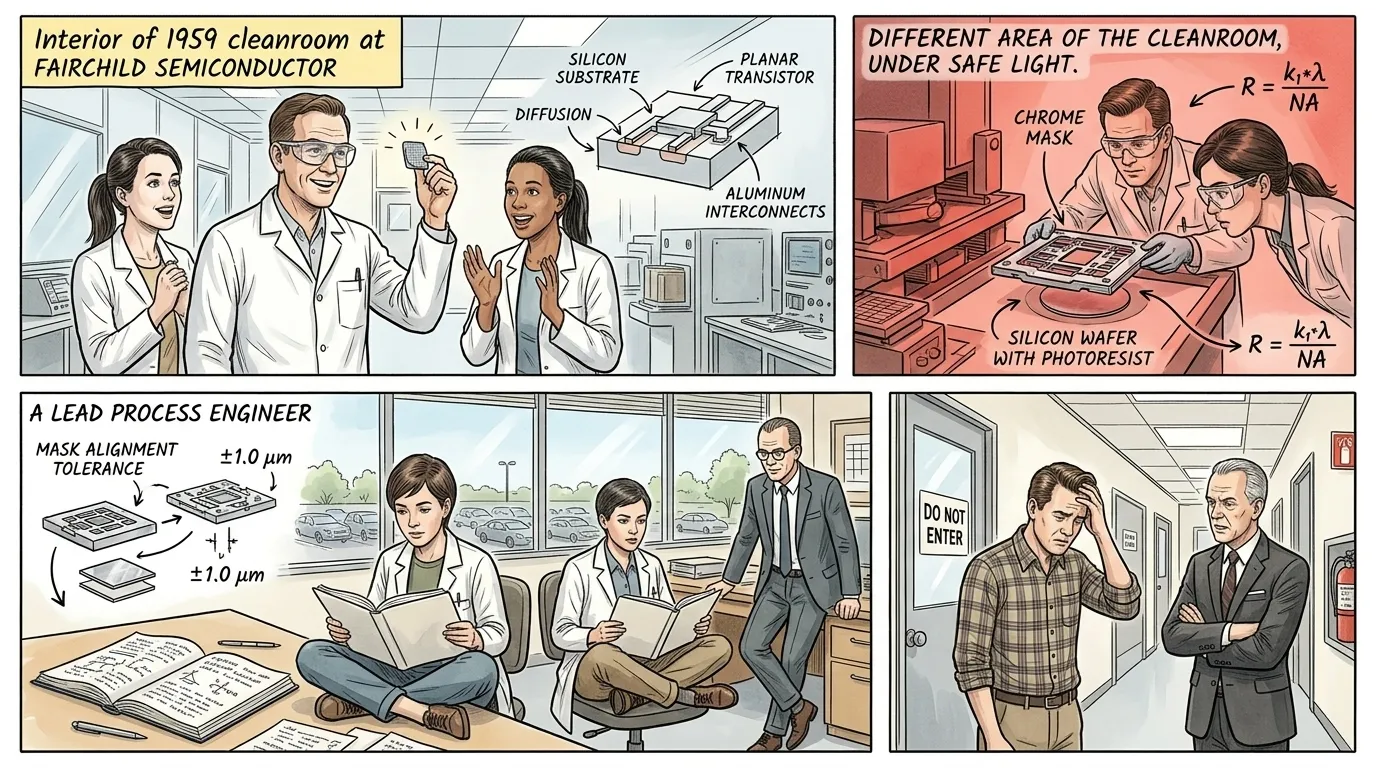
The core of modern semiconductor fabrication lies in photolithography, a process akin to photography on a microscopic scale. It begins by coating a silicon wafer with a light-sensitive polymer, or 'photoresist.' A precisely patterned mask, containing the circuit's design, is then placed over the resist. Ultraviolet light is shone through the mask, selectively hardening or softening the resist. The unexposed areas are then washed away, leaving behind a patterned stencil on the wafer's surface, ready for etching. This critical step enables the transfer of intricate designs with incredible precision.
"An experienced fabrication engineer, a man with a steady hand and protective eyewear, carefully positioned a chrome mask over a wafer. 'Precision is everything at this stage,' he explained to a trainee, a younger woman carefully observing. 'Just like a photographic negative, this mask transfers the circuit pattern onto the resist. Light etches our future, literally.'"
Page 7
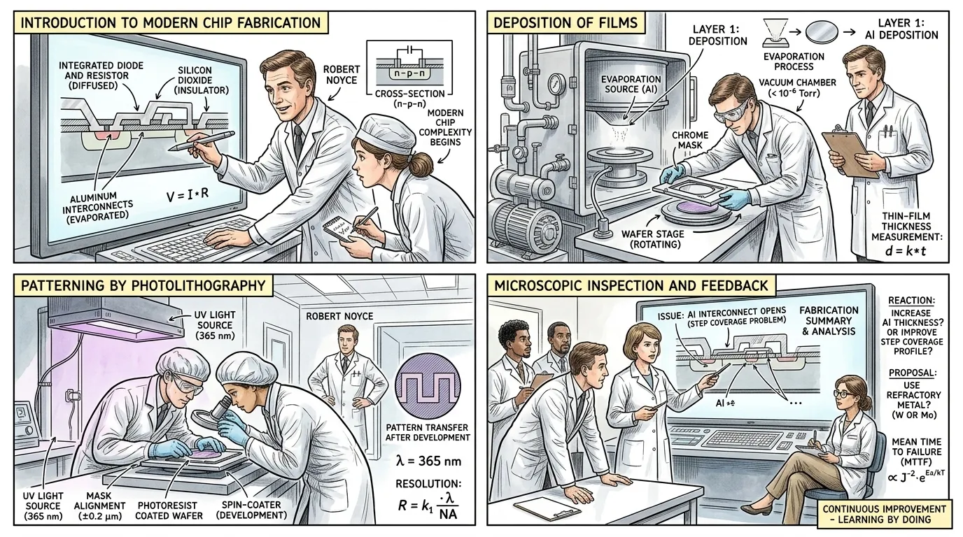
Once patterned, the wafer undergoes further transformations. 'Doping' introduces impurities into specific regions of the silicon, creating areas that conduct electricity differently, forming transistors. Then, layers of insulating materials and conductive metals are 'deposited' onto the wafer. Using subsequent photolithography and etching steps, these metal layers are patterned to create the tiny wires that interconnect the millions of transistors. This meticulous, layer-by-layer construction builds up the complex three-dimensional architecture of an integrated circuit, transforming a flat wafer into a powerful brain.
"Examining a highly magnified cross-section of a chip on a large display, a lead process engineer, a woman with short, practical hair and a focused gaze, explained to a team, 'Each layer is a critical step: first doping to define our transistors, then depositing insulating barriers, and finally, precisely patterning the metal interconnects. Layer by layer, we construct the intelligence that drives our world.'"
Page 8
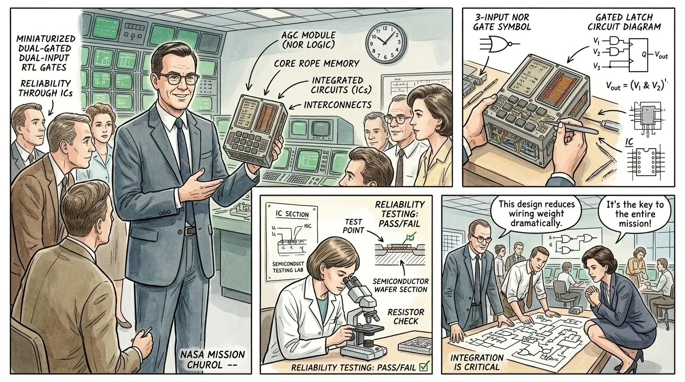
The integrated circuit swiftly moved from laboratory curiosity to a cornerstone of advanced technology. Its immediate impact was felt in applications where size, weight, and reliability were paramount. The Apollo Guidance Computer, vital for the moon landings, leveraged thousands of Kilby-Noyce style integrated circuits, allowing for unprecedented processing power in a compact, rugged form factor. Beyond space, early microchips enabled the creation of desktop calculators, transforming complex arithmetic from a room-sized endeavor to a handheld device. The era of microelectronics had truly begun.
"A proud systems architect, a man with a confident smile and spectacles, presented a module for the Apollo Guidance Computer to a group of onlookers in a 1960s NASA-style facility. 'This integrated circuit package,' he announced, 'is a marvel of compactness and reliability. It packs the power of thousands of discrete components into a space a fraction of the size. This is how we reach the moon.'"
Page 9
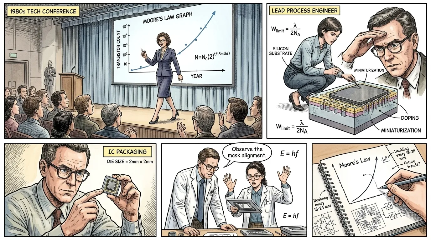
The advancement of semiconductor fabrication was not merely incremental; it was exponential. In 1965, Gordon Moore, co-founder of Intel, observed that the number of transistors in an integrated circuit would roughly double every two years, an observation that became known as Moore's Law. This self-fulfilling prophecy spurred relentless innovation in fabrication techniques, leading to ever-smaller, faster, and more energy-efficient chips. It transformed a specialized industry into a global engine of economic growth and technological progress, defying previous limits.
"A seasoned technologist, a woman with an authoritative demeanor, pointed to a projected graph depicting the upward curve of Moore's Law, highlighting various generations of microchips with their increasing transistor counts. 'The density continues to double, year after year,' she explained to a fascinated audience at a 1980s tech conference. 'This unprecedented rate of progress, fueled by improvements in fabrication, is fundamentally reshaping how humanity interacts with information.'"
Page 10
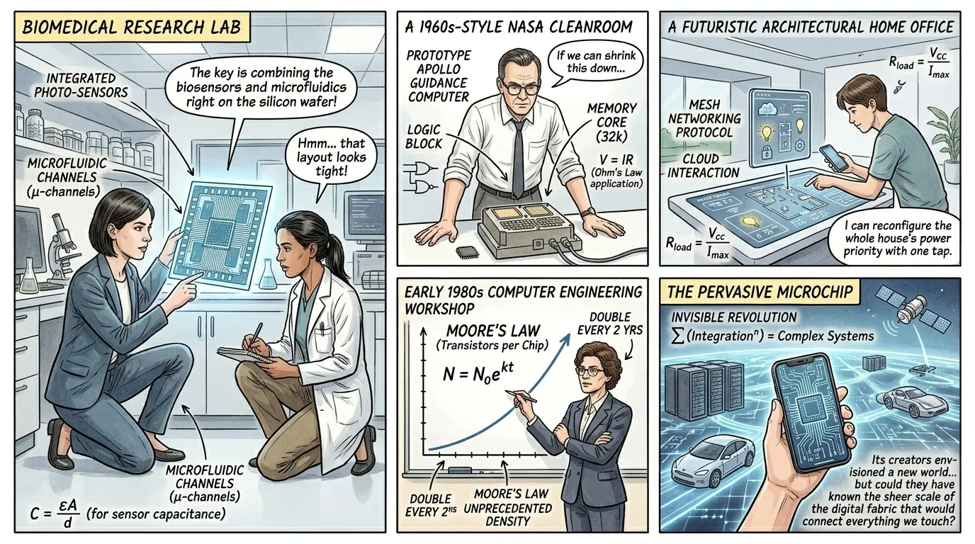
Today, semiconductor fabrication is an invisible revolution, underpinning virtually every aspect of modern life. From the supercomputers driving scientific discovery to the smartphones in our pockets, every device relies on the intricate dance of light and chemicals on silicon wafers. This complex process, born from the insights of Kilby and Noyce, continues to evolve, pushing the boundaries of what's possible in computing, communication, medicine, and energy. The microchip remains the fundamental building block of our digital age, a testament to relentless human ingenuity.
"Reflecting on the vast impact, a wise, older voice-over narrator pondered, 'We knew that we were on to something significant, but we had no idea it would affect the entire world the way it has,' quoting Robert Noyce. 'The invisible revolution whispers through every device we touch, every calculation we make, shaping a future its creators could only begin to imagine.'"
About this story
- Location: Global
- Audience: general readers
Read Wonder Inventions on your phone
Wonder Inventions is available on Android. Get Wonder Inventions on Google Play.