Transistor
Transistor — an illustrated inventions story, set in Global. 10 illustrated pages, free to read on Wonder Inventions.
Page 1
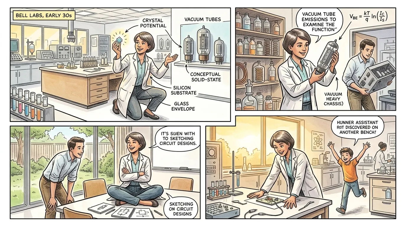
Before the advent of the transistor, the world of electronics was dominated by cumbersome, power-hungry vacuum tubes. These glowing glass bulbs, fragile and prone to failure, limited the scale and efficiency of early computers and communication systems. The relentless pursuit of smaller, more reliable components became an urgent imperative for innovation. At Bell Labs in Murray Hill, New Jersey, a dedicated team embarked on a quest that would redefine modern technology forever. Their breakthrough, a tiny solid-state device, promised to replace the bulky vacuum tube, unlocking unprecedented possibilities for miniaturization and digital processing.
""The electron tube, as then constituted, was not a satisfactory device," remarked one engineer reflecting on the era. "Its unreliability and power demands were holding back progress on an unimaginable scale. We needed a revolution, not just an evolution.""
Page 2
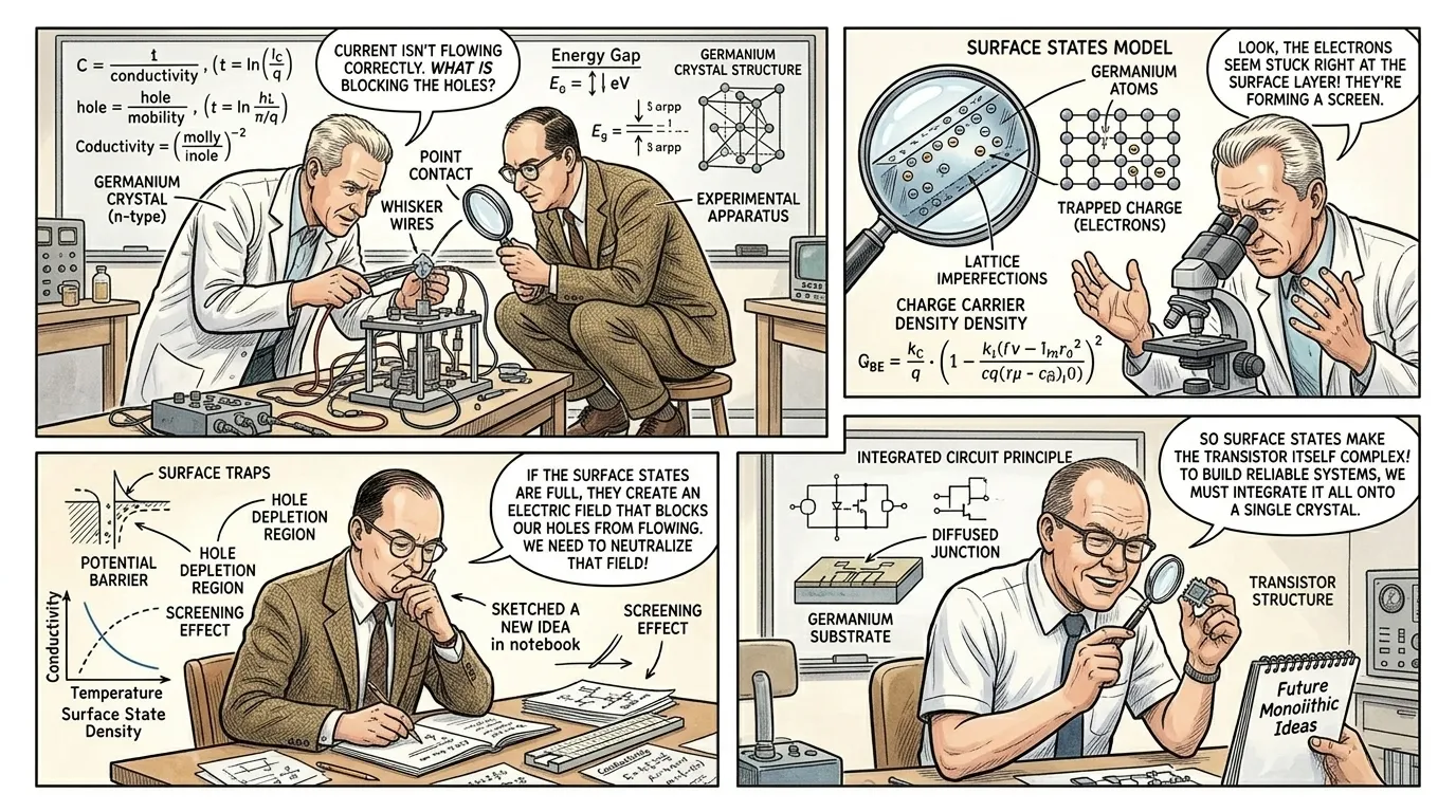
Scientists had long understood the unique properties of semiconductors, materials like germanium and silicon that conduct electricity under specific conditions, unlike metals or insulators. However, harnessing this variability to control current flow reliably proved incredibly difficult. Early attempts to build a 'field-effect transistor' were hampered by a fundamental misunderstanding of what was happening at the material's surface, where electrical signals were applied. The elusive 'surface states' often trapped electrons, preventing the desired control. It was a theoretical wall that demanded novel approaches and painstaking experimentation.
""We knew semiconductors held the key," explained one of the lead researchers in a recorded interview years later. "The theory of solid-state amplification was elegant, but the practical execution, especially controlling current at the surface, felt like trying to grasp smoke. As the ancient philosopher Aristotle once said, 'For the things we have to learn before we can do them, we learn by doing them.' We certainly had a lot of 'doing' ahead of us, and many failures.""
Page 3
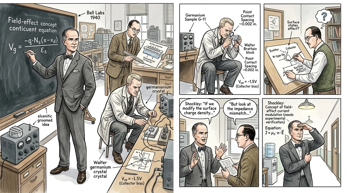
Within Bell Labs, the effort to replace vacuum tubes was a collaborative, yet sometimes competitive, endeavor. William Shockley, a brilliant physicist, pursued a field-effect approach, theorizing that an external electric field could modulate the conductivity of a semiconductor. However, his initial prototypes consistently failed due to the very surface states that John Bardeen was investigating. Bardeen, a theoretical physicist, and Walter Brattain, an experimentalist, joined forces, meticulously exploring the mysterious behavior of electrons at the semiconductor's surface. Their complementary skills would prove crucial in unraveling the true mechanism.
""Shockley's initial field-effect concepts were sound in theory," Bardeen later acknowledged in a technical paper, "but the reality of material science presented unforeseen obstacles. The surface of a semiconductor isn't a clean slate; it's a dynamic interface. Understanding that required a completely different lens. The experimental feedback from Brattain was indispensable in testing these complex theoretical models.""
Page 4
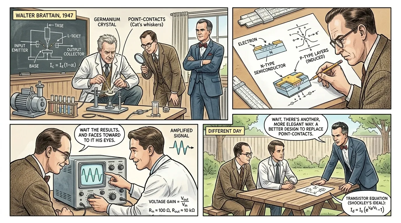
On December 16, 1947, Walter Brattain, acting on John Bardeen's theoretical insights into surface states, constructed a pivotal experiment. He placed two closely spaced gold point contacts—nicknamed 'cat's whiskers'—onto a specially prepared germanium crystal. When a small current was applied to one contact (the 'emitter'), it modulated a much larger current flowing through the other contact (the 'collector'). Suddenly, a faint input signal was amplified into a robust output. The device, crude yet undeniably functional, was the world's first working point-contact transistor, marking a monumental shift in the history of electronics.
""When we saw the amplification, a wave of profound realization swept over us," Brattain recounted in later interviews. "It wasn't just working; it was working with a gain of 18! This wasn't a minor improvement; this was a fundamental leap. It was a tangible proof that solid-state electronics could truly replace the vacuum tube. Bardeen just looked at the oscilloscope reading, a quiet affirmation in his eyes. The feeling was electric, a confirmation of years of painstaking effort.""
Page 5
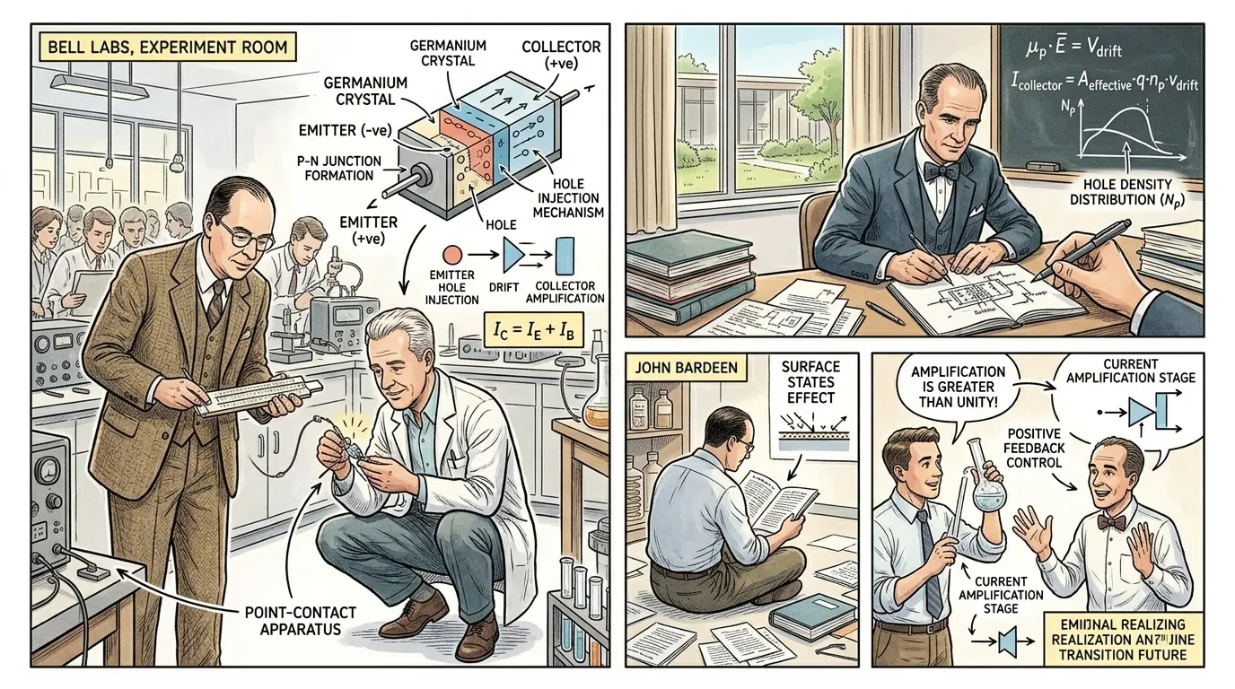
The operation of the point-contact transistor, though revolutionary, relied on a complex interplay of charge carriers. When the emitter contact injected positively charged 'holes' into the germanium, these holes were attracted to the negatively biased collector contact. However, as they moved, they also influenced the number of free electrons available in the semiconductor, effectively creating a path for a larger current to flow from the collector. A small change in the emitter current thus caused a much larger change in the collector current, resulting in amplification. It was a delicate, surface-dependent mechanism, susceptible to manufacturing variations.
""The beauty of it was in the simplicity of control," explained a physicist analyzing the early patent drawings. "A tiny input signal could open a floodgate for a much larger current. It was like steering a giant ship with a small rudder. The challenge, however, was in precisely controlling those 'holes' and electrons at the crystal surface, a phenomenon that was both powerful and frustratingly inconsistent from one device to the next.""
Page 6
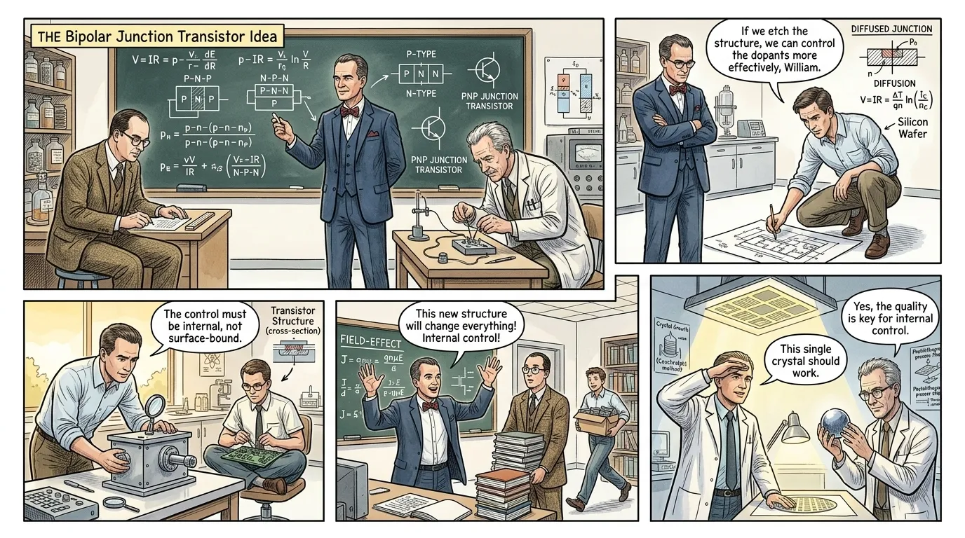
While Bardeen and Brattain celebrated their point-contact invention, William Shockley felt excluded. Driven by a desire for a more robust and elegant solution, he began working intensely on a new theoretical model. Instead of surface contacts, Shockley envisioned a 'sandwich' of semiconductor materials with different electrical properties—a P-N-P or N-P-N junction. His design, conceived largely in isolation, promised greater stability, higher efficiency, and easier manufacturing, moving the control mechanism from the unpredictable surface into the bulk of the semiconductor material. It would prove to be the practical form the transistor would ultimately take.
""I was terribly unhappy that I was left out of this," Shockley candidly admitted in his memoirs, referring to the point-contact breakthrough. "But that very dissatisfaction drove me to an even more profound understanding. The real solution lay not on the surface, but in the internal structure—in creating a reliable, controlled junction. As Mark Twain famously quipped, 'The secret of getting ahead is getting started.' But the secret of lasting impact is getting it right.""
Page 7
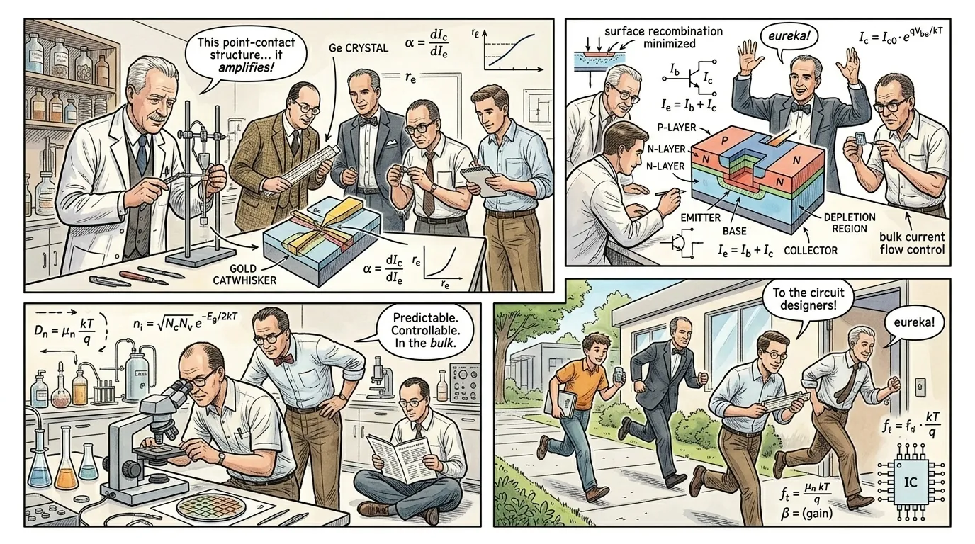
Shockley's junction transistor, often called the bipolar junction transistor (BJT), dramatically improved upon the point-contact design. By sandwiching a thin layer of P-type semiconductor between two N-type layers (N-P-N) or vice versa (P-N-P), he created a more stable and predictable device. A small current applied to the central 'base' layer could precisely control a much larger current flowing between the 'collector' and 'emitter' layers. This internal control mechanism minimized the issues of surface instability and paved the way for mass production, setting the stage for the true electronics revolution.
""The junction transistor provided a level of precision and reproducibility that the point-contact simply couldn't match," observed a Bell Labs engineer in a contemporary technical memo. "By creating these distinct, doped layers, we gained exquisite control over the flow of charge carriers through the bulk material, making the device incredibly robust and efficient. This was the design that would scale, the one that would truly change everything.""
Page 8
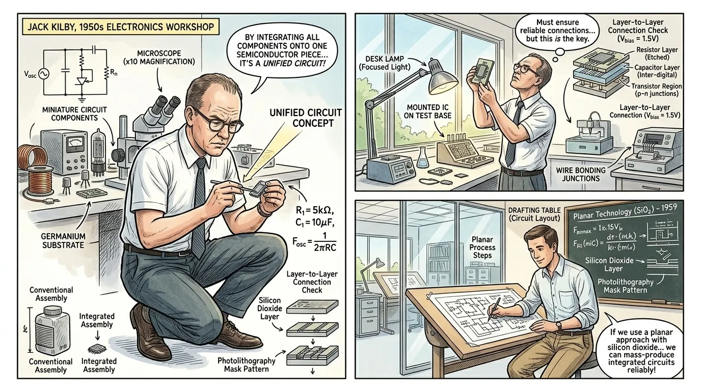
The junction transistor's inherent smallness and low power consumption opened the door to previously unimaginable miniaturization. No longer were engineers constrained by the fragile, bulky vacuum tubes. This reduction in size was not merely convenient; it was transformative, leading directly to the invention of the integrated circuit (IC) in 1958 by Jack Kilby and later, independently, by Robert Noyce. The IC packed multiple transistors and other components onto a single, tiny silicon chip, overcoming the inherent problem of connecting discrete components reliably and efficiently, a challenge identified years earlier with vacuum tubes.
""The beauty of the transistor wasn't just its function, but its scale," observed Jack Kilby in a retrospective interview. "It showed us that the limits of electronics were not in the components themselves, but in how we connected them. The integrated circuit was the logical next step, allowing us to combine thousands, then millions, of these tiny, robust switches onto a single substrate. It delivered the ultimate solution to the problem of interconnectivity, a problem that had plagued electronics since its earliest days.""
Page 9
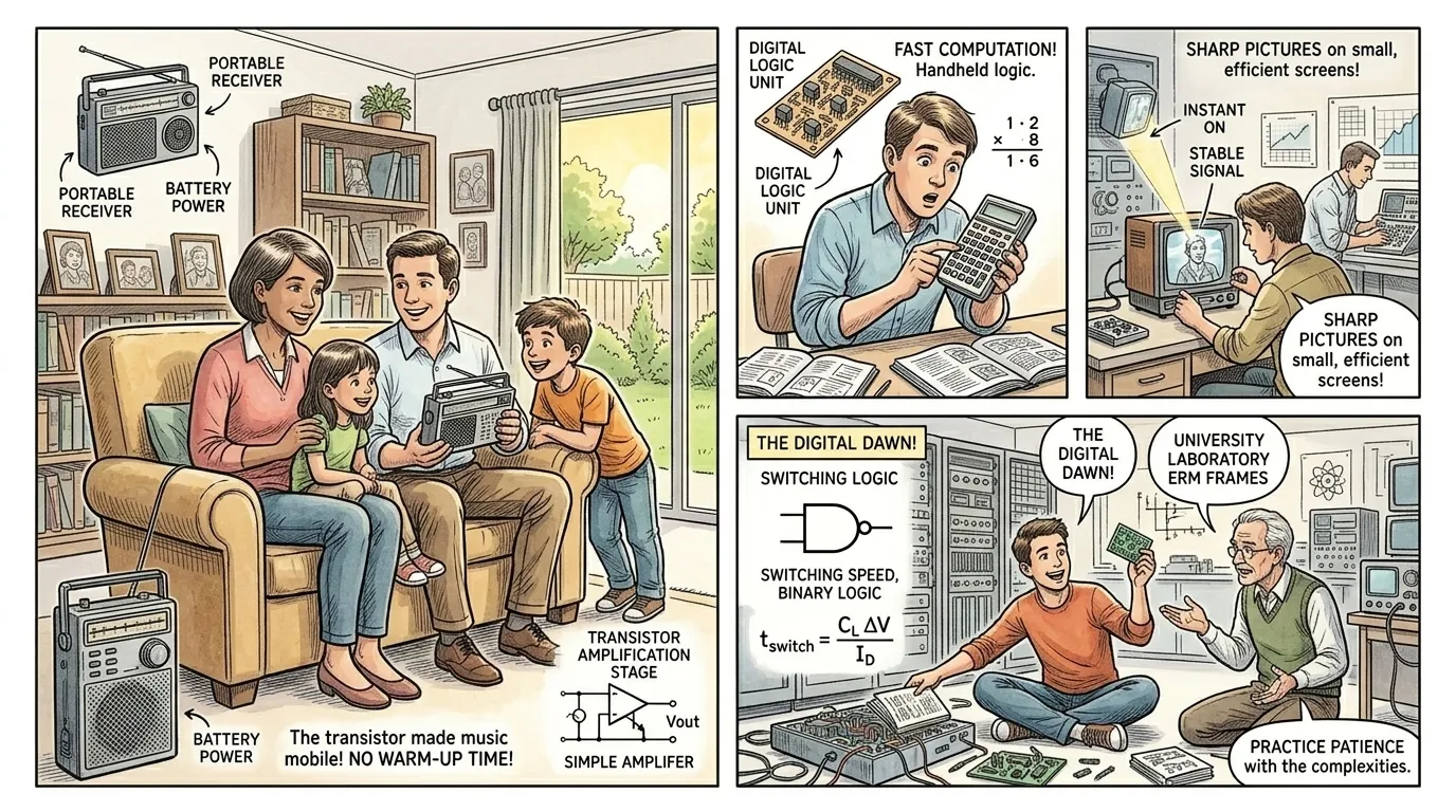
The transistor's impact rapidly permeated consumer electronics, replacing tubes in radios, televisions, and eventually, the first pocket calculators. Its reliability, efficiency, and small size made personal electronics truly portable and accessible. This widespread adoption fueled a massive expansion in the electronics industry, laying the groundwork for the digital age. From the first transistor radios to the earliest digital computers, the tiny solid-state switch became the invisible engine of technological progress, enabling complexity and sophistication previously impossible. Industries transformed, and daily life began an irreversible shift towards an interconnected, electronic future.
""The transistor did more than just replace a component; it redefined an industry," stated a prominent electronics historian in a documentary. "It democratized access to computation and communication. As the pioneering computer scientist Grace Hopper often said, 'The most dangerous phrase in the language is, 'We've always done it this way.'' The transistor absolutely shattered 'always done it this way,' opening up entirely new paradigms for how technology could serve society.""
Page 10
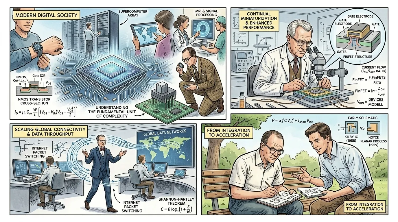
Today, the transistor remains the fundamental building block of virtually all modern electronics. Billions of transistors are fabricated onto every microchip, powering everything from the smallest smartwatch to the most powerful supercomputer. It enables the vast global communication networks, artificial intelligence, medical diagnostic tools, and the very internet that connects us. The seemingly simple act of controlling electron flow in a solid-state material, pioneered by Bardeen, Brattain, and Shockley, unleashed a cascade of innovation that continues to define and reshape human civilization. Its legacy is etched into every digital interaction, a testament to the profound power of scientific inquiry and inventive genius.
""The transistor is more than just an invention; it's the invisible foundation of the modern world," remarked a leading nanotechnology researcher. "Its principles, refined over decades, continue to push the boundaries of what's possible in information processing and connectivity. As the great scientist Albert Einstein famously pondered, 'The important thing is not to stop questioning.' The transistor itself stands as a monumental answer to a question, but it has also enabled an infinite number of new questions for humanity to explore.""
About this story
- Location: Global
- Audience: general readers
Questions and answers
Read Wonder Inventions on your phone
Wonder Inventions is available on Android. Get Wonder Inventions on Google Play.